


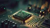


Combination of ultra-thin high-density silicon capacitors and power supply network (BSPDN) on the ba


This invention combines Ultra-Thin High-Density Silicon Capacitors (UTHDSC) with a Backside Power Supply Network (BSPDN) specifically for the 2nm semiconductor node. It addresses power stability and noise issues by embedding high-capacitance, low-ESR/ESL capacitors on the wafer's backside. This ensures stable voltage delivery and reduces power loss, enabling high-performance AI and computing chips to operate more efficiently within smaller device footprints.
At the 2nm node, extreme transistor density and fast switching speeds create significant power supply noise and voltage instability. Traditional front-side power delivery causes "routing congestion" where signal and power lines compete for space, leading to significant "IR drop" (voltage loss). Moreover, conventional capacitors are too bulky and suffer from high leakage currents at high temperatures, which compromises the reliability and energy efficiency of advanced processors.
The solution embeds UTHDSCs directly into the Backside Power Supply Network. By moving power delivery to the wafer's backside and placing capacitors closer to the transistors, it minimizes the power path length. These capacitors use advanced dielectrics to mitigate leakage and feature low ESR/ESL to provide near-instantaneous voltage compensation. This suppresses high-frequency noise and stabilizes the 2nm chip's performance while supporting thinner, high-density wafer-level fan-out (WLFO) packaging.
It addresses the "Power Delivery Bottleneck" and "Signal Interference" caused by traditional front-side routing. In prior art, as scaling reaches 2nm, power loss becomes unmanageable due to routing density. This invention resolves the physical conflict between power and signal lines through backside integration and overcomes the limitations of traditional capacitors regarding bulkiness and high-temperature leakage at the nano-scale.
- 2nm Process Compatibility: Tailor-made for high-density transistor environments.
- Low Equivalent Inductance (ESL) and ESR: Achieve extremely fast noise suppression and power response.
- Back-mounted Technology: Saves valuable front-side wiring space and improves signal integration.
- Leakage Current Suppression: Utilizes advanced dielectric materials to ensure energy-efficient operation at high temperatures.
- Package Integration Support: Seamlessly integrates with wafer-level fan-out (WLFO) packages, reducing module size.
Industries where the invention can be useful?
High-performance computing (HPC): Large data center servers. Artificial intelligence (AI): Generative AI training and inference processors. Mobile communications: 5G base station power amplifiers and flagship mobile phone chips. Autonomous driving systems (ADAS): High-performance sensors and computing modules for vehicles.An estimate of the total addressable market?
$13000000Potential Customers/End Users. Who might benefit?
Wafer foundries: TSMC, Samsung, Intel. Fabless semiconductor companies: NVIDIA, AMD, Apple, Qualcomm. OSAT (Outsourced Semiconductor Assembly and Test) companies: ASE and other companies specializing in advanced packaging.Documents
-
1766221465529_665.pdf
Actions
Added all portfolio
| Country | Current Status | Patent Application Number | Patent Number | Applicant / Current Assignee Name | Title | Google Patent Link |
| Taiwan | Issued | M668047 | TWM668047U | Dollarchip Technology Inc. | Combination of ultra-thin high-density silicon capacitors and backside power supply network in 2nm process | Google patent link |
You may also like the following patent
Combination of Ultra-Thin High-Density Silicon Capacitors and Fan-out Packaging Glass Substrate
| Available For: Taiwan | Semiconductors and Electronics |
This innovation combines Ultra-Thin High-Density Silicon Capacitors (UTHDSCs) with fan-out packaging glass substrates to enhance electrical performance. By embedding UTHDSCs within or near the...
| Application Number | M669584 |
| Patent Number | TWM669584U |
| Current Status | Issued |